slot machine write-up (Google CTF 2017 Finals)
“slot machine” was a hardware task in the reverse-engineering category on Google CTF Finals 2017, which took place in Zurich back in October 2017.
All teams got the same ATtiny-based slot machine game, which contained 2 stub flags. The objective was to reverse-engineer it by disassembling it (in literal real-life sense) and dumping the firmware, figure out how flags can be obtained without access to the circuit, and do that with the machine at the organizers’ table, which contained the real flags.
You get:
- Slot machine game
- Printed schematics with some hints and instructions (instructions, schematics)
- Screwdriver
- Small prototyping breadboard
- USBasp programmer
- Several jumper cables
The set of provided tools suggests several things.
USBasp programmer means that we’re probably going to deal with AVR family microcontroller. For instance, popular Arduino Uno is based on AVR microcontroller.
The programmer has the ability to download the firmware (unless it was read-protected through so-called fuse bits), so that’s probably exactly what we’re going to do.
Let’s inspect the game first.
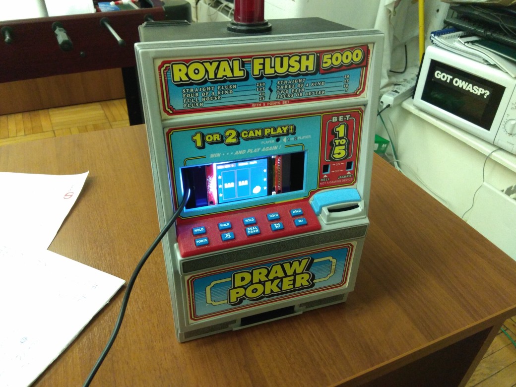
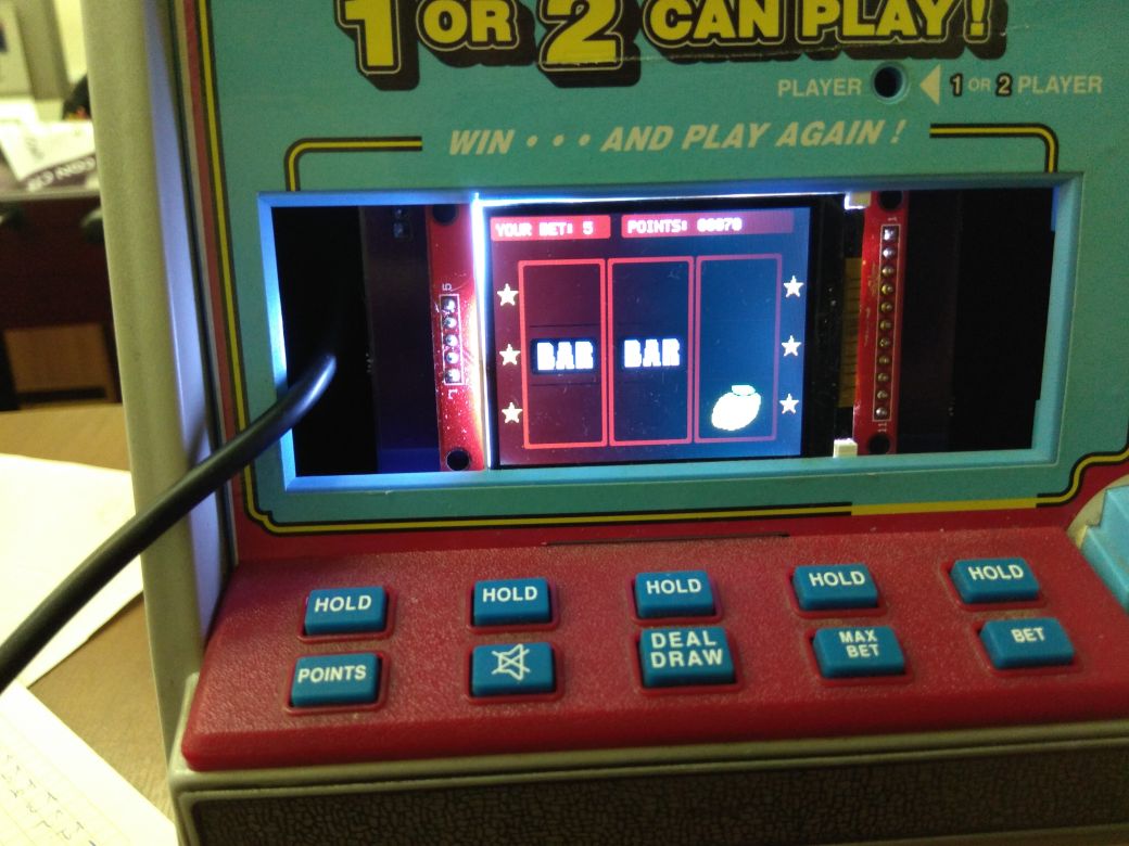
The slot machine has an LCD screen, like those commonly used in various DIY Arduino projects, and can be found cheaply on AliExpress.
Out of 10 buttons, only 2 from the upper row appear functional and, according to the schematics, the lower row is not connected at all. Pressing the leftmost button cyclically changes the current bet from 1 to 5. Pressing the second button plays the game. At the start of the game, you have 100 credits.
The game works like a typical slot machine. At the center of the screen, there are three reels, which display random symbols each time game is played: nothing, “bar”, lemon, and “7”. Having three matching symbols in a row will give you some credits based on your bet.
However, at that point, the conditions to get the flags were not yet known.
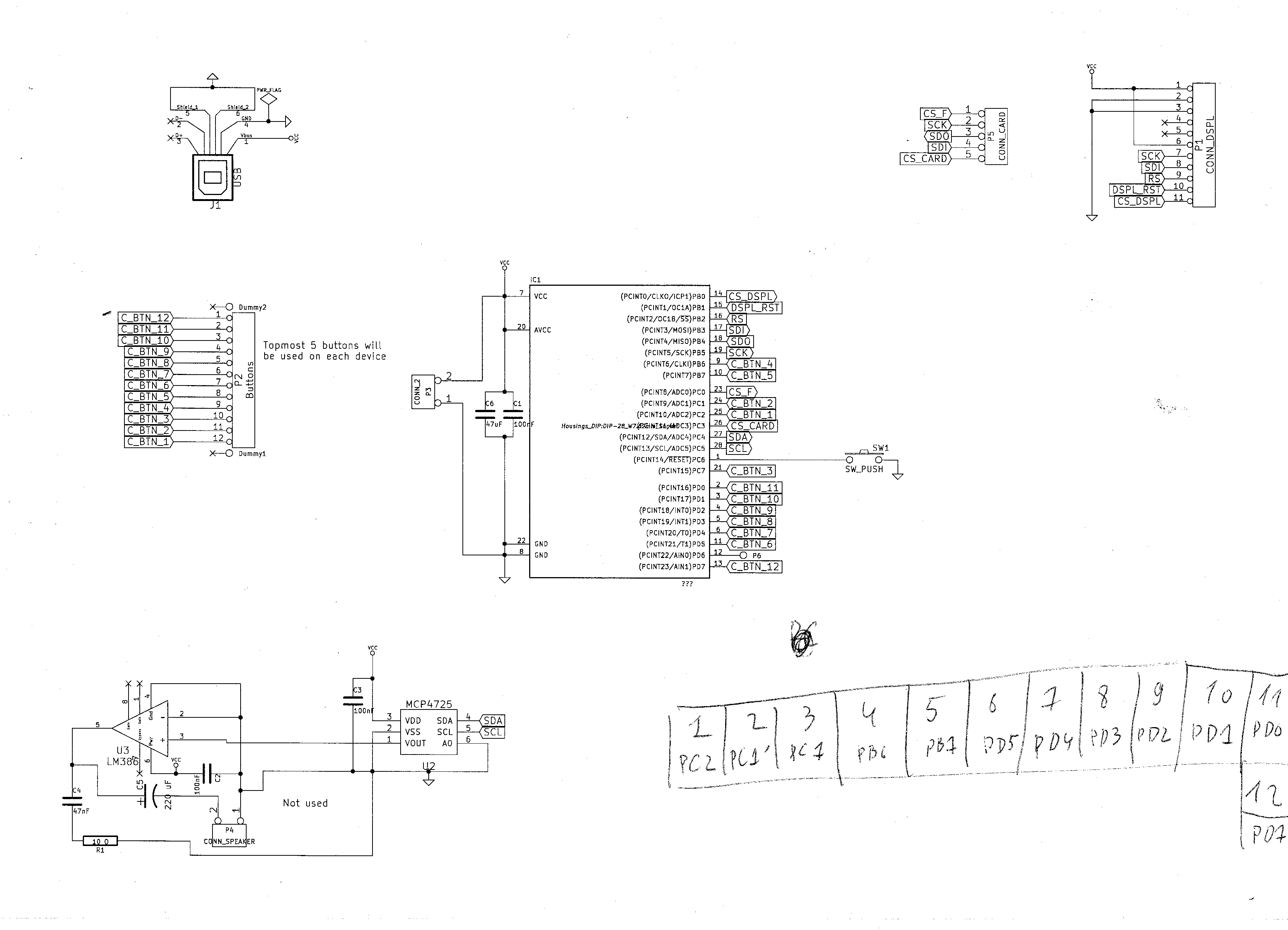
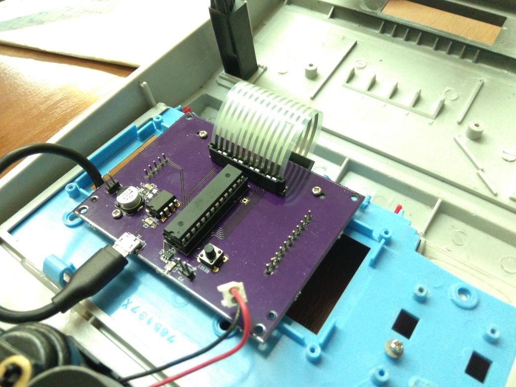
So, without much hesitation, I disassembled the slot machine. What was inside is a printed circuit board with ATtiny88 microcontroller.
ATtiny is one of the less powerful microcontrollers in AVR family. Although all AVR microcontrollers share the same basic instruction set (there are some instruction extensions, though), they have different set of integrated peripherals, like timers, IO ports, SPI interfaces, and so on.
The programmer uses simple protocol called ISP (in-system programming) over Serial Peripheral Interface to talk to the microcontroller.
In order to figure out how to connect the programmer to the MCU, we need to consult with the datasheet.
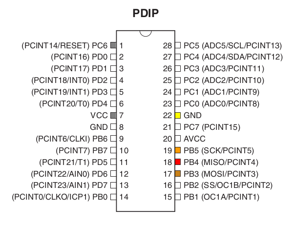
MISO (master in, slave out), MOSI (master out, slave in), SCK (serial clock), RST (reset), VCC (+5 volts) and GND (ground) must be connected to the corresponding ouputs of the programmer.
Since these outputs are not exposed on the PCB, microcontroller IC had to be removed from its socket and inserted into the breadboard.
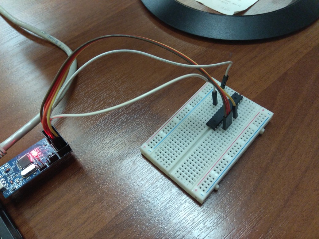
Once it’s done, it’s easy to dump the firmware using avrdude program. It wasn’t read-protected after all, so there were no problems dumping it.
avrdude -c usbasp -p t88 -U flash:r:slot_machine.bin:r
You can download the file here.
Reverse-engineering
Processor selection
AVR processors are relatively well-supported by IDA disassembler. Although there’s no Hexrays decompiler support, disassembler works mostly fine, but there are still some annoying problems.
One the of the major obstacles is CPU selection dialog.
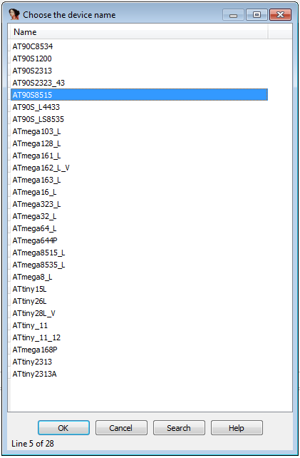
Although all processors in the AVR family have the same basic instruction set, as it has been mentioned above, they have different set of integrated peripherals and amount of available memory.
Selecting device with mismatching memory size will result in either truncated code section or buggy data section references (or both).
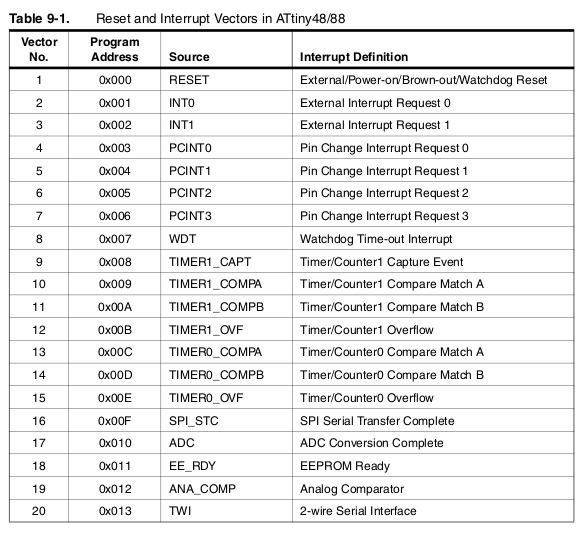
The set of peripherals affects two twings: IO registers and interrupt vectors.
The registers tend to occupy the same location across all AVR family. That is, locations corresponding to missing peripheral will be described as “reserved” in the datasheet, and remaining registers will be “fragmented” instead of “compacted”.
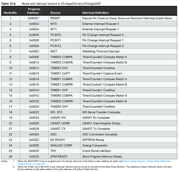
However, interrupt vector layouts are very different. There are no unused vector numbers (which is likely caused by the fact that it would waste precious flash memory otherwise). For example, compare interrupt vectors on ATtiny88 and ATmega328p.
It wouldn’t be much of a problem if IDA actually had definitions for all the AVR processors. Unfortunately, as you can see on the screenshot, it isn’t the case. So the best option seems to select the best matching processor (which one is the best matching is also not obvious), and fix incorrect things (like interrupt names) by hand, consulting with the processor reference manual.
.data section
Another problem lies in how .data section is initialized.
To understand the problem, let’s first discuss C and compilers in general.
.data section is where initialized data in your program goes to. In C, that would be all non-zero initialized variables with static lifetime (i.e. global variables and static variables inside functions). There’s also .rodata section for things like string constants (AFAIK there’s no memory protection in AVR, so there’s no dedicated .rodata either).
How do these variables get from the executable file to the RAM?
On typical desktop Linux, this is handled by the ELF parser with the aid of MMU: ELF parser maps the corresponding regions of the ELF file with copy-on-write access rights. This operation is transparent, and the description of the .data region - where it lies in the binary and where it should be mapped - can be easily parsed from the ELF file.
There comes a little caveat. There’s usually no ELF parser in embedded devices. And no MMU, either. There’s just a blob of code in the flash storage, where the only thing you know for certain is entry point address.
How is .data section handled in this case?
In the avr-libc (which is a commonly used C library for AVR), there’s a small piece of code that’s executed right after reset, just before calling user’s main function.
What this code does is it copies initial values for .data section from the persistent flash memory to RAM. These initial values are stored simply appended at the end of .text (code) section.
Let’s take a look at the assembly code.
For the people unfamiliar with AVR assembly, a couple of points:
- Data and code space are separate.
- AVR executes code from flash memory directly. Instructions are word-addressable, 1 word = 2 octets (16 bits total).
- AVR cannot execute code from RAM at all. It’s a Harvard architecture processor (purists will still find a couple of places where it deviates from pure Harvard architecture, though).
- Flash memory can be read-accessed using special
lpminstruction. Besides.datainitialization, it’s often for string constants and various tables, because there’s much more flash memory available than RAM on (probably) all AVR devices. There are even special versions of typical libc functions that operate on data located in the program memory instead of RAM: pgmspace.h, snprintf_P. Unlike program counter,lpminstruction is byte-addressable. - Flash memory can also be programmed by the MCU itself using
spminstructions. It’s often used by bootloaders, like the one flashed on Arduino Uno that programs sketches received via serial interface from the USB chip. It’s completely irrelevant for our discussion here, but I think it’s worth mentioning. - Since all registers are 8 bit in size, but memory address width is 16-bit, register pairs are used to access arbitrary memory addresses. They are
X(r26-r27),Y(r28-r29) andZ(r30-r31).
ROM:034D __do_copy_data:
ROM:034D                 ldi     r17, 1          ; Load Immediate
ROM:034E                 ldi     r26, 0          ; X = 0x0100 (RAM:0100)
ROM:034F                 ldi     r27, 1          ; Load Immediate
ROM:0350                 ldi     r30, 0xA6       ; Z = 0x19A6 (ROM:0CD3)
ROM:0351                 ldi     r31, 0x19       ; Load Immediate
ROM:0352                 rjmp    loc_355         ; Relative Jump
ROM:0353 ; ---------------------------------------------------------------------------
ROM:0353
ROM:0353 loc_353:                                ; CODE XREF: __RESET+10↓j
ROM:0353                 lpm     r0, Z+          ; Load Program Memory
ROM:0354                 st      X+, r0          ; Store Indirect
ROM:0355
ROM:0355 loc_355:                                ; CODE XREF: __RESET+B↑j
ROM:0355                 cpi     r26, 0xDE       ; Compare with Immediate
ROM:0356                 cpc     r27, r17        ; RAM:01DE
ROM:0357                 brne    loc_353         ; Branch if Not Equal
In this fragment, data is copied from Z = 0x19A6 (byte offset for the program memory) to X = 0x0100 (byte offset for RAM) until X becomes 0x01DE.
In order to see the data in IDA, you’ll need to copy the data manually. The following IDA Python script will do that for you:
DATA_START = 0x0100
DATA_LENGTH = 0x01DE - DATA_START
DATA_PROGMEM_BYTE_OFFSET = 0x19A6

IDA_VIRTUAL_RAM_BEGIN = 0x100000

assert DATA_PROGMEM_BYTE_OFFSET % 2 == 0, "fix this script a bit"

for i in xrange(0, DATA_LENGTH, 2):
    # in IDA, AVR ROM memory has 16-bit words, so
    # 1) Byte() returns 16-bit values
    # 2) byte offset must be divided by two to get 16-bit word offset
    val = Byte((DATA_PROGMEM_BYTE_OFFSET + i)//2)

    val0 = val & 0xFF
    val1 = val >> 8

    PatchByte(IDA_VIRTUAL_RAM_BEGIN + i + DATA_START, val0)
    PatchByte(IDA_VIRTUAL_RAM_BEGIN + i + 1 + DATA_START, val1)
Actual reverse-engineering
Now that we’re set, let’s finally dive into the code.
Of course, I’m unable to reproduce the exact sequence of actions I did to figure out the program flow. Neither would it be practical due to rather chaotic nature of reverse-engineering process.
However, one of the first things I noticed certainly was the flag strings:
RAM:01A7	{FLAG_II}
RAM:01B1	{FLAG_I}
We can start from there.
Here comes another problem with IDA and AVR assembly. AVR is 8-bit processor having (up to) 16-bit addresses. So when constant address is passed to the function, it’s stored in register pair using two load instructions. IDA can’t recognize this pattern, and cross-references for data don’t work as is.
I had to resort to searching for individual bytes of the addresses using “Search -> immediate value…”.
There were two fragments of the code mentioning addresses of the two flags:
ROM:0A32                 ldi     r24, 0xB1       ; Load Immediate
ROM:0A33                 ldi     r25, 1          ; Load Immediate
ROM:0A34                 rjmp    loc_BB4         ; Relative Jump
They both lead to function that display “Congratulations!” and the flag on the screen.
The flag addresses don’t seem to appear anywhere else, so we’re likely looking in the right place.
Tracing the code graph upwards, I found the following code:
ROM:0A14                 lds     r24, unk_1001DE ; Load Direct
ROM:0A16                 cpi     r24, 9          ; Compare with Immediate
ROM:0A17                 brne    dispatch_start  ; Branch if Not Equal
ROM:0A18                 sts     unk_1001DE, r1 ; Store Direct to SRAM
ROM:0A1A                 movw    r30, r2         ; Copy Register Word
ROM:0A1B                 ldi     r22, 0x4C ; 'L' ; Load Immediate
ROM:0A1C                 ldi     r23, 1          ; RAM:014C
ROM:0A1D                 ldi     r18, 0x43 ; 'C' ; Load Immediate
ROM:0A1E                 ldi     r19, 1          ; RAM:0143
ROM:0A1F                 ldi     r24, 1          ; Load Immediate
ROM:0A20                 ldi     r25, 1          ; Load Immediate
ROM:0A21
ROM:0A21 loc_A21:                                ; CODE XREF: main+201↓j
ROM:0A21                 ld      r20, Z+         ; Load Indirect
ROM:0A22                 movw    r26, r22        ; Copy Register Word
ROM:0A23                 ld      r21, X+         ; Load Indirect
ROM:0A24                 movw    r22, r26        ; Copy Register Word
ROM:0A25                 cpse    r20, r21        ; Compare: Skip if Equal
ROM:0A26                 ldi     r25, 0          ; Load Immediate
ROM:0A27                 movw    r26, r18        ; Copy Register Word
ROM:0A28                 ld      r21, X+         ; Load Indirect
ROM:0A29                 movw    r18, r26        ; Copy Register Word
ROM:0A2A                 cpse    r20, r21        ; Compare: Skip if Equal
ROM:0A2B                 ldi     r24, 0          ; Load Immediate
ROM:0A2C                 cp      r30, r4         ; Compare
ROM:0A2D                 cpc     r31, r5         ; Compare with Carry
ROM:0A2E                 brne    loc_A21         ; Branch if Not Equal
ROM:0A2F                 tst     r25             ; Test for Zero or Minus
ROM:0A30                 brne    flag1           ; Branch if Not Equal
ROM:0A31                 rjmp    loc_BE4         ; Relative Jump
ROM:0A32 ; ---------------------------------------------------------------------------
ROM:0A32
ROM:0A32 flag1:                                  ; CODE XREF: main+203↑j
ROM:0A32                 ldi     r24, 0xB1       ; Load Immediate
ROM:0A33                 ldi     r25, 1          ; arg1 = RAM:01B1
ROM:0A34                 rjmp    loc_BB4         ; Relative Jump
unk_1001DE is incremented each time any button is pressed. So every time user presses buttons 9 times in any order, check_secret_sequence loop executes.
The loops compares some array that lies on the stack with RAM:014C and RAM:0143. These two static arrays contain [4, 3, 2, 1, 0, 1, 2, 3, 4] and [0, 1, 0, 1, 4, 3, 4, 3, 2] correspondingly. Interesting…
Intuition suggested that it’s some secret key combination, and that array on the stack contains last 9 pressed buttons.
And the intuition was indeed correct, pressing buttons in order (0 being the leftmost button, and so on) specified by the second array gave me the first flag.
Predicting the random generator
The second secret combination is more insteresting.
It opens so-called developer menu that allows user to advance pseudorandom number generator (PRNG) state by almost any arbitrary number.
I bet most of you have heard the story about hackers that predicted the internal state of actual real-life slot machine PRNG to get advantage and win money reliably (though I haven’t actually heard the story until after solving this task :)).
The second part of the task is pretty much the reenactment of that story.
Although the initial state of PRNG seems to be truly random, the PRNG itself is rather weak. It’s just linear congruential generator with 32 bits of state, driven by equation state = state * 0x41C64E6D + 31337.
Even though I couldn’t trace the exact code path that leads to the second flag, intuition once again suggested that in order to obtain the second flag, triple “7” must be rolled.
rand() function is called 9 times per every game, once for each symbol on the screen. Symbols are determined in column-major order, that is, the left reel comes first (from top to bottom), then the middle reel, and finally the right reel.
Each symbol has some fixed probability. It can be expressed as the following pseudo-code:
int next_symbol(void) {
    uint16_t val = rand();
    if (res >= 0xFD70) return SEVEN;
    if (res >= 0xF0A3) return LEMON;
    if (res >= 0xBAE0) return BAR;
    return EMPTY;
}
It leads to the following idea: play a couple of games, take notice of which symbols are rolled, then brute-force the internal state of the generator. Although the brute-force will be probabilistic, the longer the sequence is, the higher chance there is only one such initial state. In practice, playing 5 games is more than enough to reliably find the state value.
With current internal state known, it’s now easy to find the number that must be added to the current state in order to get the state where triple “7” will be rolled immediately.
Brute-force program and most of the PRNG reverse-engineering work was done by my teammate vient.
You can check out the program here.